Edge contacts of graphene formed by using a controlled plasma treatment
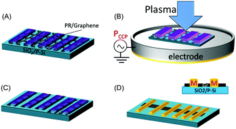
Despite the fact that the outstanding properties of graphene are well known, the electrical performance of the material is limited by the contact resistance at the metal–graphene interface. In this study, we demonstrate the formation of “edge-contacted” graphene through the use of a controlled plasma processing technique that generates a bond between the graphene edge and the contact metal. This technique controls the edge structure of the bond and significantly reduces the contact resistance. This simple approach requires no additional post-processing and has been proven to be very effective. In addition, controlled pre-plasma processing was applied in order to produce CVD-graphene field effect transistors with an enhanced adhesion and improved carrier mobility. The contact resistance attained by using pre-plasma processing was 270 Ω μm, which is a decrease of 77%.

http://pubs.rsc.org/en/content/articlelanding/2014/nr/c4nr05725b#!divAbstract


