- Equipment
- Home > Introduction > Equipment
E-beam lithography Draw fine patterns (0.2 μm ~ 1800 μm)
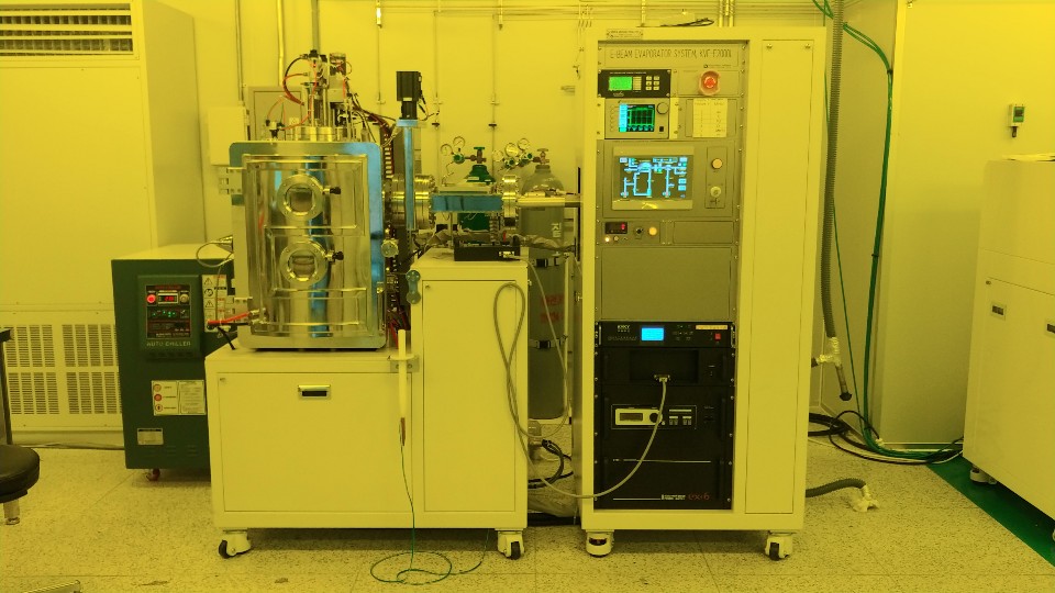
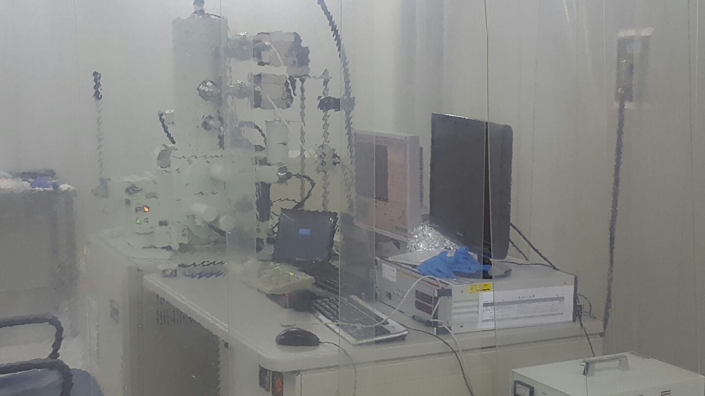
E-beam depositionDeposit various metals (Ti, Cr, Pd, Au, Pt, Ag, Cu, Ni, Co)
IV/CV analyzerMeasure IV or CV by agilent 4155C
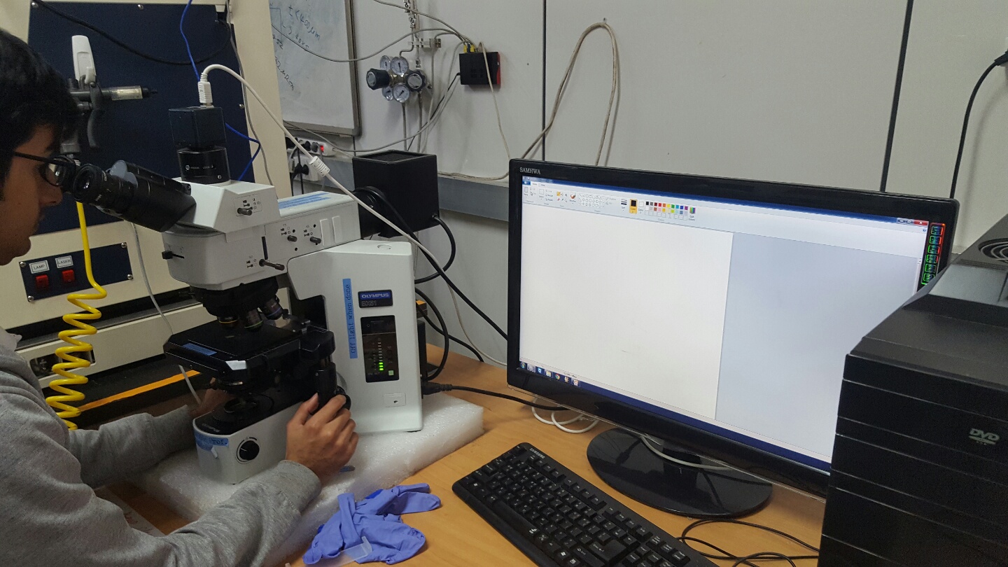
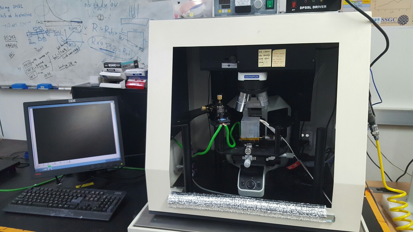
Optical microscopySee optical images (x25 ~ 1000)
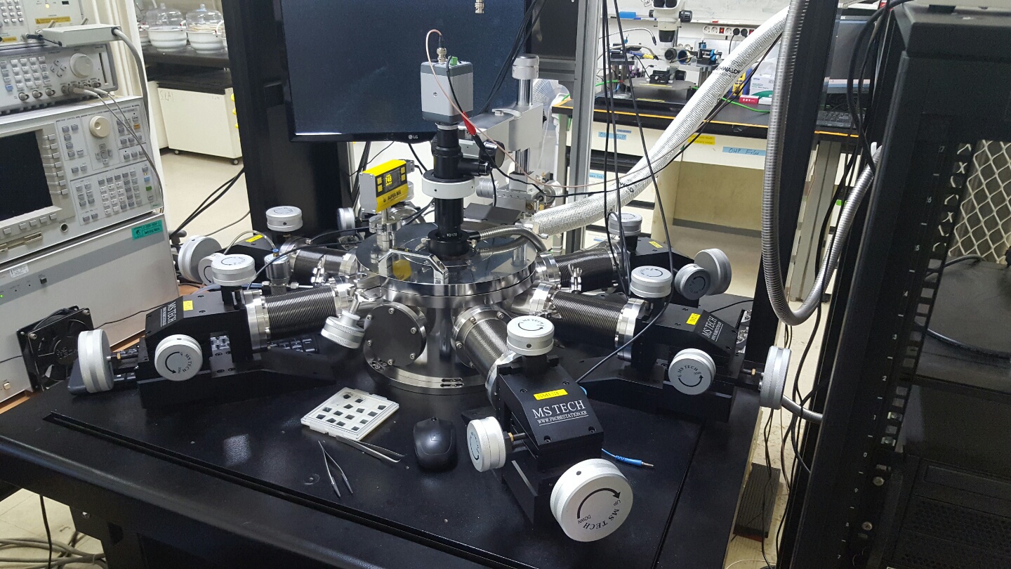
2D material stackingStack various 2D materials
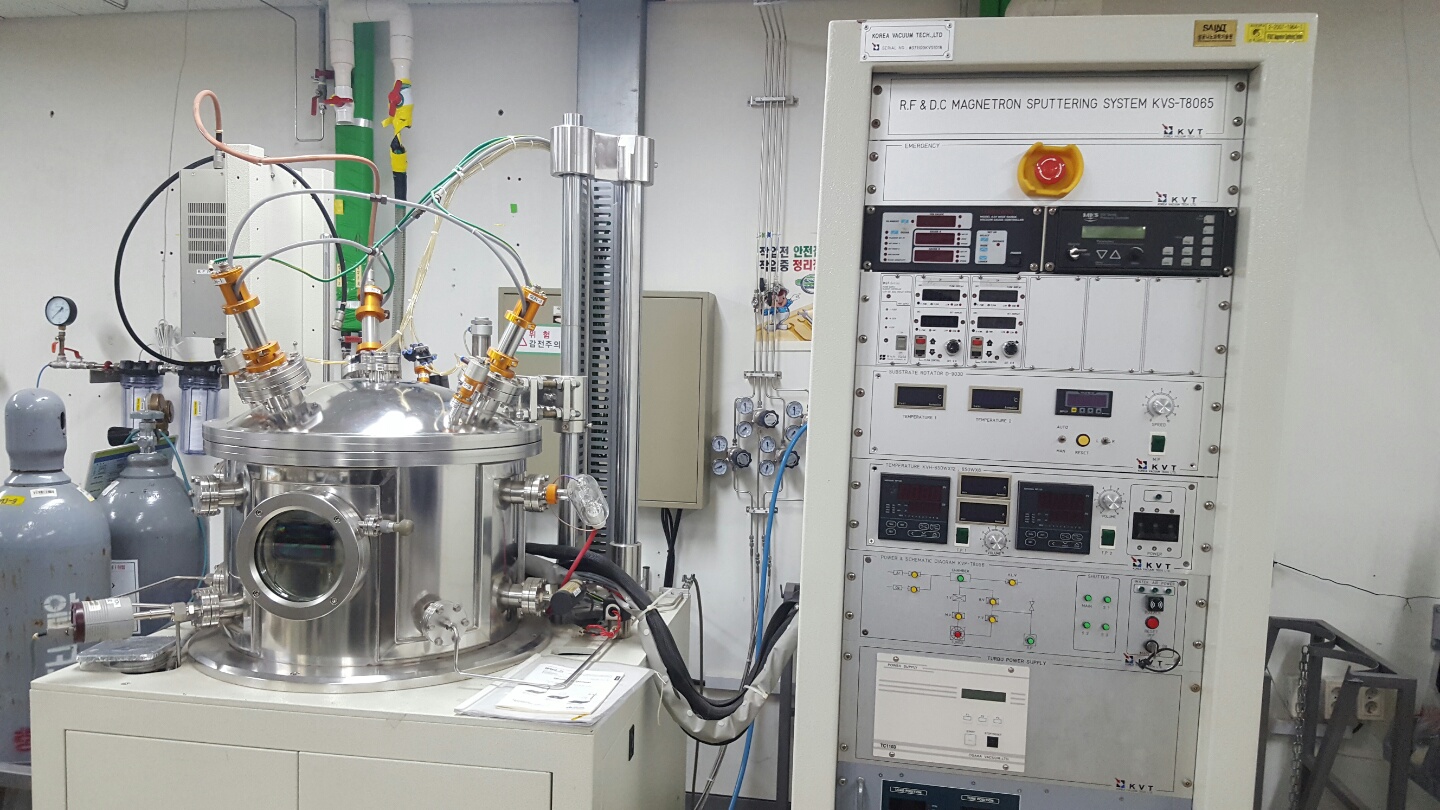
SputterSputtering
Reactive ion etcherPlasma etching by RIE method
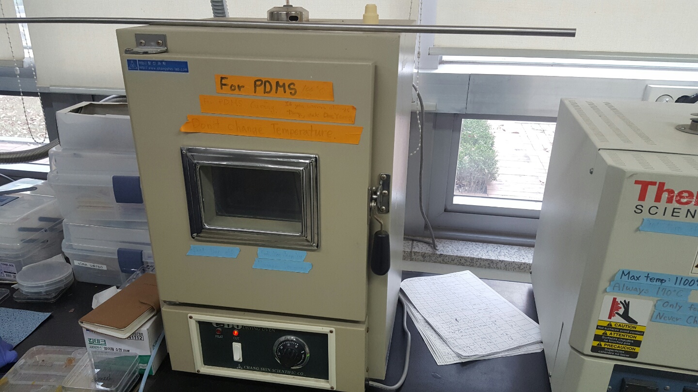
OvenOven (RT ~ 300 ℃)
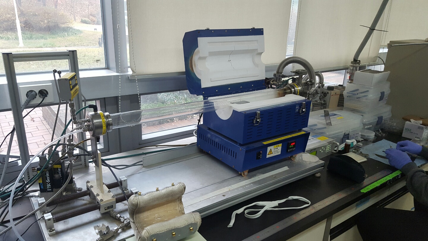
Thermal CVDThermal CVD (RT ~ 1100 ℃, @ few mtorr)
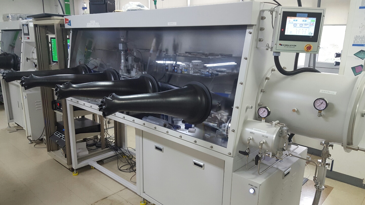
Glove boxSample treatment in Nitrogen ambient
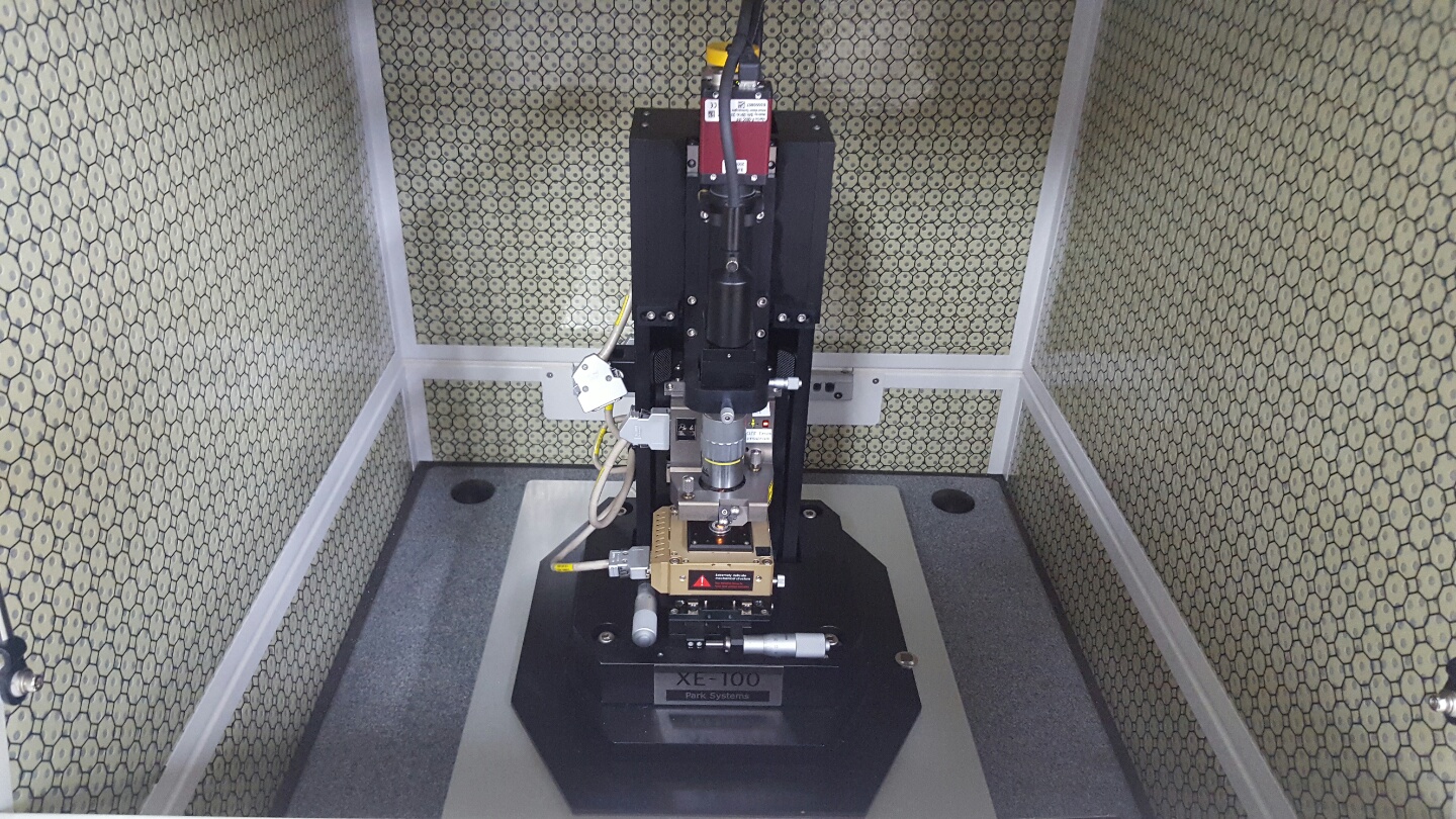
AFM&KPFMMeasuring atomic thickness
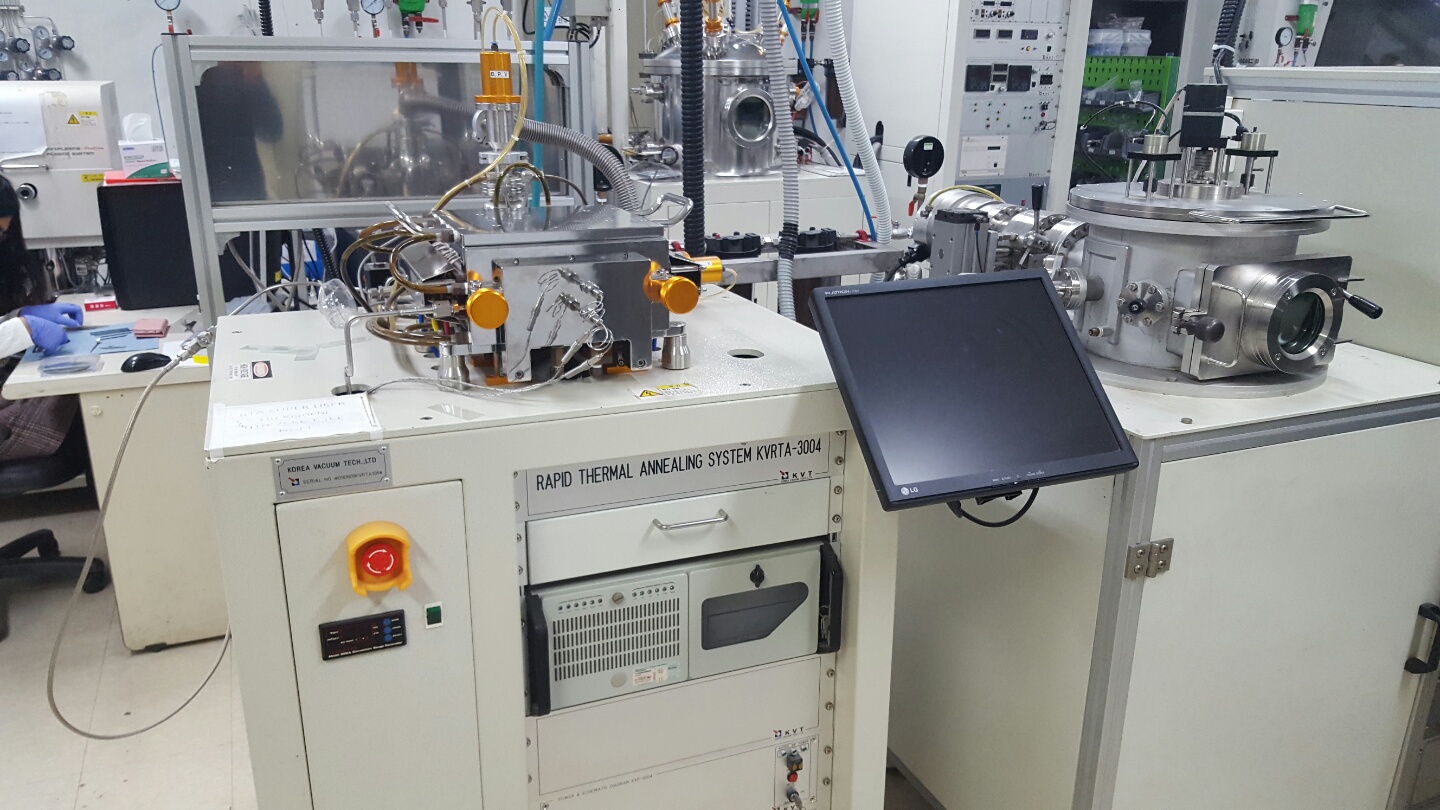
Rapid thermal annealingRapid thermal annealing
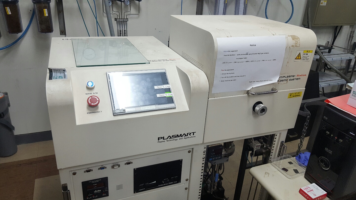
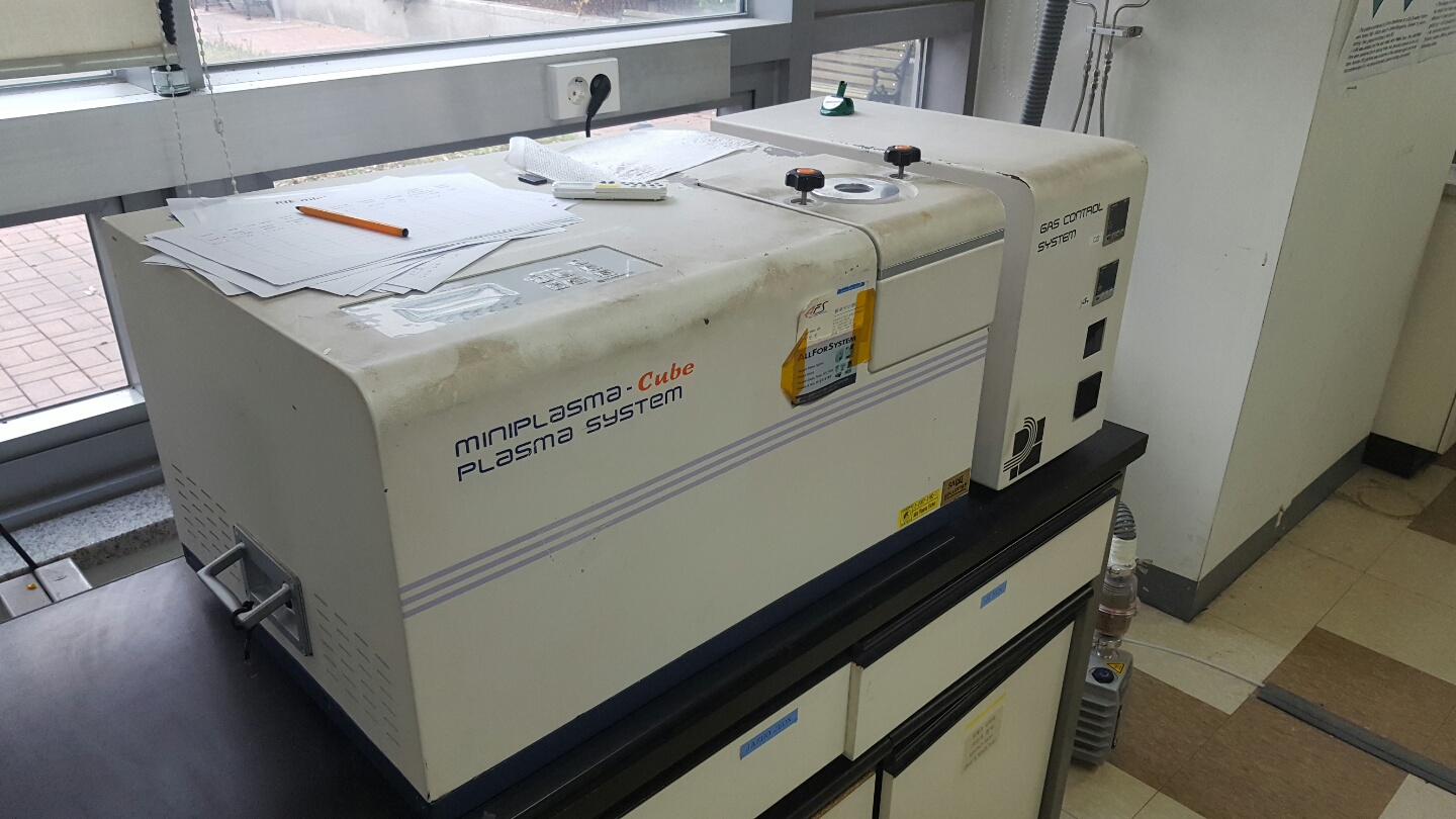
ICP/CCP plasmaPlasma etching by ICP or CCP method
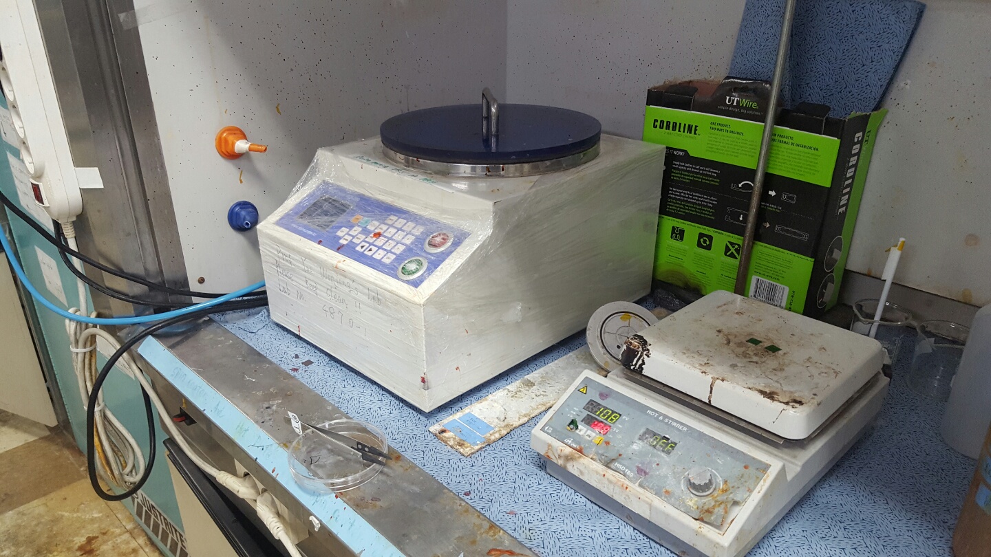
Spin coater & hot plateSpin coating
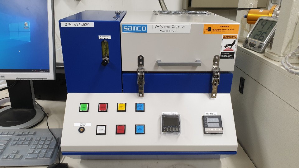
UV-1 Ozone CleanerOzone treatment with UV
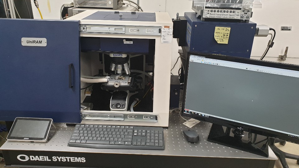
Raman spectroscopyMeasure raman shifts of materials
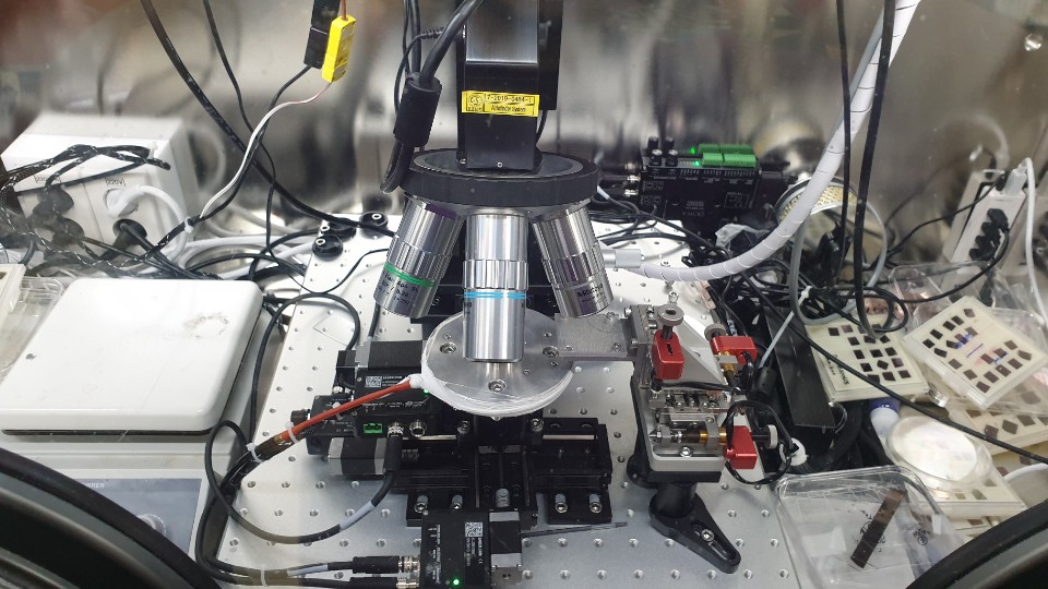
AutofinderUsing for finding and stakcing 2d materials in a glovebox
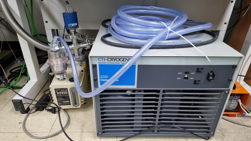
CryostatReaching very low temperature

 E-MAIL